

Modern civilization demands energy, and the energy demand is increasing almost every day all over the world. The dependency on conventional energy resources including fossil fuel, oil, gas, coal etc. are not in favor of having sustainable global earth. For this reason, renewable or clean energy is one only option while acquiring energy from the […]
IS09 – Collision Dynamics of Solitons in a Grating Assisted Semilinear dual-core System with Phase Mismatch
The collision dynamics between two counterpropagating moving Bragg grating solitons and their outcomes in a model of semilinear dual-core Bragg-grating coupler with phase mismatch are investigated. The influence of gratings phase mismatch on the collision outcomes is also discussed.
LD06 – Relative intensity noise of injection-locked epitaxial quantum dot laser on silicon
This work investigates the relative intensity noise (RIN) characteristics of quantum dot (QD) lasers epitaxially grown on silicon subject to the optical injection. The effect of threading dislocation (TD), which acts as nonradiative recombination centers in the Shockley-Read-Hall (SRH) process, is considered in the rate equation model. The results reveal that the RIN is enhanced […]
IS01 – Network Authentication with Synchronized Chaotic Lasers
We numerically study a hardware method for network authentication, where a pair of matched (twins) chaotic lasers generate the same chaos when they synchronize, being subject to the same optical injection from a third chaotic laser. One of the lasers is in the secure environment, the other in the unsecure environment, and authorization is granted […]
N09 – Beam shaping using a chain of photonic nanojet induced plasmonics
Photonic nanojet arises from a microcavity leading to high electric field. On the other hand, metal nanoparticles (NPs) lead to high field due to localization in small volumes. In this work, PNJ from an array of cavity induced plasmon resonances has been studied. The sharp profile of the PNJ has been observed by the inclusion […]
LD09 – Simulation of the Spectral Behavior in High-Power Distributed Feedback Lasers above Threshold
We report on the simulations of mode hopping behavior in semiconductor distributed feedback lasers with asymmetric facet reflectivities above threshold and its dependence on the phase between the grating and the high reflective facet.
IS05 – Thermal crosstalk mitigation in a dual-drive Mach-Zehnder Modulator
Dual-drive, PIN-diode based Mach-Zehnder modulators are pivotal for power-efficient and cost-effective CMOS compatible optical transceivers with small footprints. However, the basic chip materials have substantial thermal conductance resulting in thermal crosstalk, which eventually deteriorates the modulator performance in terms of bandwidth and data transmission capabilities. In this work, we simulate and analyze the influence of […]
P12 – Design and Simulation of Temperature Sensors Based on Thermo-Optical WGM Shifts in Silica and Non-Silica Glass Microcavities
Sensing applications of dielectric microcavities with whispering-gallery modes (WGMs) have been actively studied in the recent years. Here we investigated theoretically temperature microsensors based on different glasses, including common silica glass, as well as special germanate, tungsten-tellurite, arsenic sulfide and arsenic selenide glasses. We developed numerical model describing sensing characteristics of the considered microcavities. We […]
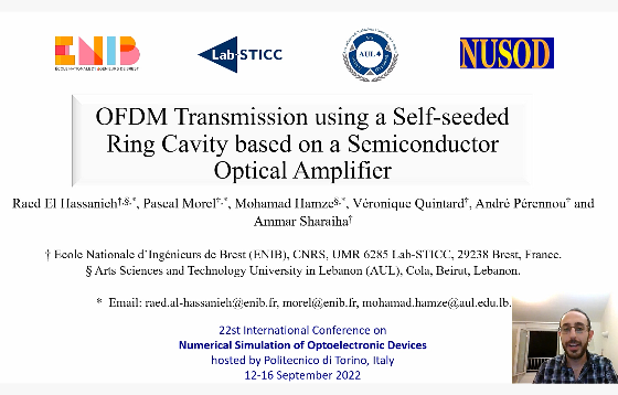
IS07 – OFDM Transmission using a Self-seeded ring Cavity based on a Semiconductor Optical Amplifier
This paper discusses the transmission of optical Orthogonal Frequency-Division Multiplexing (OFDM) format modulation in a resonant cavity based on a Semiconductor Optical Amplifiers Fiber Cavity Laser (SOA-FCL). The OFDM Subcarriers are configured and transmitted to fit the Cavity Resonance Modes (CRM). As a result, the authors show a novel principle of OFDM transmission in a […]
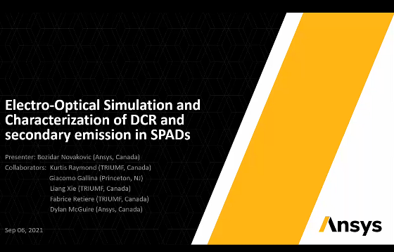
D02 – Electro-Optical Simulation and Characterization of DCR and secondary emission in SPADs
We demonstrate the use of simulations in the modeling and characterization of important aspects of Single Photon Avalanche Detectors (SPADs). Electrically, we discuss the use of drift-diffusion and avalanche triggering probability solvers and results for dark count rate (DCR) and their comparison to measurements. Optically, we discuss the use of full wave electromagnetic solvers to […]
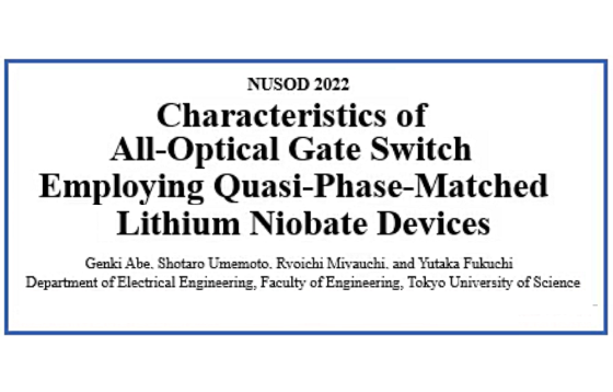
IS06 – Characteristics of All-Optical Gate Switch Employing Quasi-Phase-Matched Lithium Niobate Devices
We analyze characteristics of all-optical switches using the cascade of second harmonic generation and difference frequency mixing in quasi-phase-matched lithium niobate devices. Numerical calculations consider not only the pulse waveforms but also the optical noises.
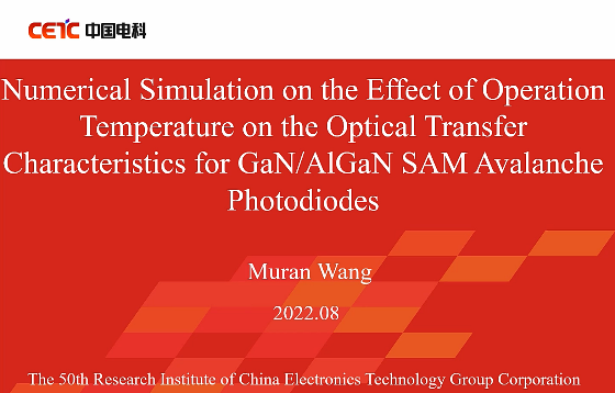
D08 – Numerical Simulation on the Effect of Operation Temperature on the Optical Transfer Characteristics for GaN/AlGaN SAM Avalanche Photodiodes
GaN/AlGaN avalanche photodiodes (APDs) have important application values and broad application potentials in the field of solar-blind ultraviolet (UV) detection. However, the self-heating effect has an obvious influence on the output characteristics of GaN/AlGaN APDs. In order to study the influence of self-heating temperature on its performance, the numerical model of GaN/AlGaN APDs is established […]
P13 – Genetic algorithm optimization of infrared plasmonic absorbers
The absorption of a multiband absorber based on a periodical plasmonic grating has been optimized. The optical and geometrical parameters of the plasmonic structure which is composed of germanium and gold are determined by an efficient genetic algorithm. The electromagnetic response of the absorber is numerically obtained by using the frequency domain finite element method. […]
D05 – Mode-Guided Infrared Absorption in Ge/SiO2 Grating for Large-Angle and Broadband Photodetection
The numerical simulation of the electromagnetic properties of the Ge/SiO2 grating structure with bottom distributed Bragg reflector. With mode guiding in Ge, the structure exhibits an absorption angle of 100° and broadband behavior from 1300 to 1500 nm.
IS04 – All-optical AND Logic Gate Based on Semiconductor Optical Amplifiers for Implementing Deep Recurrent Neural Networks
The development of optical logic gates is a key factor for enabling next generation of computations in the context of Deep Learning and Quantum Computing. In this work, we introduce a scheme for the implementation of an all-optical AND logic gate, which makes use of semiconductor optical amplifiers (SOA) in cross-phase modulation configuration combined with […]
N03 – Band structures in highly strained 3D nanowires
We mathematically derive a new nonlinear strain model to simulate the conduction and valence bands in highly bent 3D hexagonal nanowires with GaAs core and asymmetric (AlαIn1-α)As stressor. The model is based on a transformation of the 1st Piola-Kirchhoff stress tensor and an appropriate energy functional that captures the dynamics of the induced strain due […]
IS08 – Flat-band 8-Channel Optical MUX/DeMUX for Long Reach 400GbE Applications
We propose novel optical demultiplexer scheme for LR-8 applications, and theoretically verify flatband spectral response with the discrete 8-channel wavelengths. By the additional band rejection filter, non-continuous wavelength filtering response was achieved with spectral flatness and low crosstalk of < -15dB within an entire LR-8 targeted spectral range.
P09 – 120° Hybrid for Bimodal Interferometers
An 120° hybrid for bimodal interferometers in the 220 nm silicon-on-insulator technology is presented. Three output signals enable an unambiguous phase detection over a 360°-range as well as a constant sensitivity. The length of the hybrid is only 190 µm with a simulated excess loss of 0.16 dB. Measurements combined with digital signal processing verify […]
LD07 – Physics-based time-domain modeling of VCSELs
This paper presents the results of a physics-based time-domain simulator for a vertical-cavity surface-emitting laser (VCSEL). We implemented a trapezoidal rule second order backward differentiation formula (TR-BDF2) to simulate the large signal response of the device under investigation, including the parasitic effects of the pin junction arising from an interplay of optical and carrier transport […]
MM09 – FiPo FDTD: Computational Electrodynamics Technique Producing Both Fields and Potentials
We present the field–potential finite-difference time-domain (FiPo FDTD) algorithm, which solves a set of first-order equations for the electric and magnetic fields (E and H), as well as the magnetic vector potential A and the scalar electric potential φ in the Lorenz gauge. We also present the derivation and implementation of a convolutional perfectly matched […]
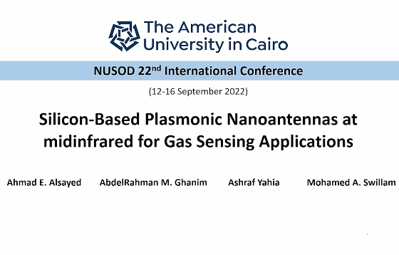
NM08 – Silicon-Based Plasmonic Nanoantennas at midinfrared for Gas Sensing Applications
Advanced nanotechnology especially CMOS technology- enables us to re-design the classic antenna in the nanoscale, which can convert propagating optical wavelengths instead of radio and microwave wavelengths into localized energy and vice versa. As a result, sensors may be designed to make sensing molecules with their characteristic vibrational transitions easier. Bowtie silicon nanoantennas are investigated […]
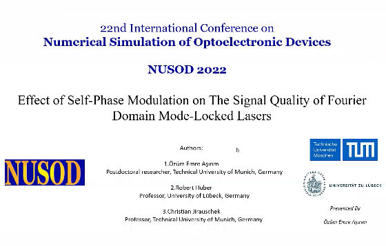
LD10 – Effect of Self-Phase Modulation on The Signal Quality of Fourier Domain Mode-Locked Lasers
In this paper, the impact of self-phase modulation on the noise performance of Fourier Domain Mode-Locked (FDML) lasers is investigated. It is shown that under a relatively high fiber nonlinearity and/or intracavity signal amplitude, an excess amount of noise generation occurs, which can not only lead to poor signal quality, but also operational instability. Hence, […]
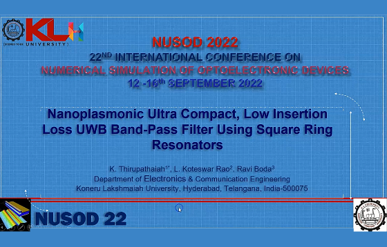
P23 – Nanoplasmonic Ultra Compact, Low Insertion Loss UWB Band-Pass Filter Using Square Ring Resonators
This article presents the design and analysis of a nanoplasmonic ultra wide band (UWB) band-pass filter based on metal insulator metal (MIM) slot-waveguide using three square ring resonators (SRRs) for obtaining ultra wide band nature at optical frequencies. This filter shows the low insertion loss due to the zero coupling gaps and no mismatch between […]
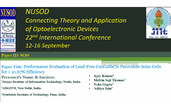
SC04 – Performance Evaluation of Lead-Free Cs2CuSbCl6 Perovskite Solar Cells for > 21.67% Efficiency
This work investigates the performance of Cs2CuSbCl6-based lead-free perovskite solar cells for photovoltaic applications. Cs2CuSbCl6 has a bandgap of 1.7eV and it is a durable and non-toxic material. Cs2CuSbCl6 can absorb more photons and thus obtain high efficiency. This work has been performed using SCAPS-1D software with the focus on optimizing the absorber layer thickness […]
IS14 – Tunable optical mode converter based on SOI asymmetric channel waveguides
An optical mode converter based on asymmetric dual channel waveguides is reported and analyzed. The first channel is infiltrated with nematic liquid crystal (NLC) material while the second one has BK7 glass core. The first higher order mode of the NLC core is coupled to the fundamental mode of the neighboring core with high coupling […]
D03 – 3D multiphysics transient modeling of vertical Ge-on-Si pin waveguide photodetectors
We report transient simulations of Ge-on-Si vertical pin waveguide photodetectors (WPDs), where the optical generation term used by the time-domain model is the FDTD solution of the electromagnetic problem treated as a spatially-distributed pulsed signal. This approach, validated against experimental measurements of the frequency response, paves the way to future studies of the dynamic response […]
NM15-Performance Optimization of Surface Plasmon Resonance based Sensors from the First Principle
Performance optimization of surface plasmon resonance (SPR) based sensors due to improvement in input optical coupling is theoretically investigated from the first principle. Various design parameters are optimized in a typical prism coupling Kretschmann configuration.
LD13 – Numerical Analysis of Electrically Pumped SiGeSn/GeSn Quantum Well Transistor Laser
The threshold current density of electrically pumped Sn incorporated group IV alloy based transistor laser (TL) is analyzed by proposing and designing a theoretical model for the same. Active region for the lasing action is formed by strain compensated GeSn single quantum well (QW) in the base of the transistor. The threshold current density for […]
NM01 – Machine Learning Assisted Material and Device Parameter Extraction From Measurements Of Thin Film Semiconductor Devices
The simulation of thin film semiconductor devices is challenging, partly due to the unknown material and device parameters. In this contribution, we present two different approaches to determine the missing material and device parameters from measurements. They both have in common that they are based on machine learning (ML) and numerical models. First, a numerical […]
SC02 – Numerical simulation of eco-friendly 4-terminal all perovskite tandem solar cell using novel HTL structure in the bottom sub cell
In this paper, we proposed a free-pb 4-terminal (4T) all perovskite tandem solar cell (APTSC) as reference with the power conversion efficiency (PCE) of 26.42% . First, a 100 nm MgF2 thin film is used as an antireflection layer (ARL) of the top sub cell to improve the total PCE of the reference structure. The […]

