

Compound semiconductor heterostructures such as quantum dots, nanowires, or thin films, are commonly subject to randomly fluctuating alloy compositions if they contain ternary and quaternary alloys. These effects are obviously of an atomistic nature and thus rarely considered in heterostructure designs that require simulations on a continuum level for theory-guided design or interpretation of observations. […]
LD04 – Modeling carrier transport in mid-infrared VCSELs with type-II superlattices and tunnel junctions
Vertical-cavity surface-emitting lasers are promising light sources for sensing and spectroscopy applications in the midinfrared 3 ÷4 µm spectral region. A type-II superlattice active region is used for carrier injection and confinement, while a buried tunnel junction defines a current aperture, decreasing the series resistivity. Highly nanostructured to optimize device performance, mid-infrared VCSELs pose modeling […]
MM04 – Simulation of ac conductivity of monolayer MoS2 at terahertz frequencies
We present a multiphysics numerical tool for calculating the terahertz (THz) conductivity of transition-metal dichalcogenides (TMDs). The tool combines the ensemble Monte Carlo (EMC) technique for carrier transport with a three-dimensional finite-difference-time-domain (FDTD) solver for electromagnetic fields. We use the coupled EMC–FDTD technique to calculate the frequency-dependent conductivity in the terahertz range for monolayer MoS2, […]
LD02 – Microscopic modeling of interface roughness scattering and application to the simulation of quantum cascade lasers
The theory of interface roughness (IFR) scattering in semiconductor heterostructures is well established in the case of idealized abrupt interfaces. However, in reality, interfaces have a finite width, i.e. interfaces are graded. In such case, the effect of interface roughness, i.e. the breaking of in-plane invariance, a general framework has been lacking to describe the […]
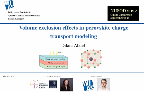
MM07 – Volume exclusion effects in perovskite charge transport modeling
Due to its flexibility, perovskite materials are a promising candidate for many semiconductor devices. For example, Perovskite Solar Cells (PSCs) have become recently one of the fastest growing photovoltaic technologies. In this work, we take volume exclusion effects into account by formulating two different current densities – either treating the mobility or the diffusion as […]
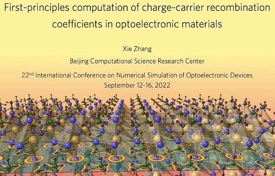
LED01 – First-principles computation of charge-carrier recombination coefficients in optoelectronic materials
Charge-carrier recombination plays a decisive role in determining the efficiency of optoelectronic materials and devices, but their accurate experimental measurements and interpretation are challenging. In this context, first-principles computation of charge-carrier recombination coefficients is particularly useful. It allows not only rigorous computation of the recombination rates, but also intuitive interpretation of the microscopic recombination mechanisms […]
LED07 – Effect of Parabolic Quantum Well on Internal Quantum Efficiency of InGaN/GaN based MicroLED at low current density
The quantum cascade stark effect (QCSE) in rectangular shaped quantum well (QW) poses a hindrance to increase the internal quantum efficiency (IQE) of nitride based LEDs. To circumvent the said problem for micro-LEDs operating at low current density, a parabolic QW structure has been proposed which is found to be useful to alleviate the QCSE […]
LD11 – Single Transverse Mode Operation of Over 10 µm Wide Ridge-Type Semiconductor Lasers with Transversal Diffraction Gratings Tatsuhiro Hirose and Takahiro Numai
This paper reports on single transverse mode operation of a ridge-type semiconductor laser with transversal diffraction gratings for a mesa width over 10 µm when the number of periods is 160, the grating pitch is 428.7 nm, and the grating depth is 250 nm.
IS10 – Modelling and Characterisation of Silicon Waveguides in Photonic Integrated Circuits
Modelling and characterization of basic waveguiding structures in integrated photonics is important due to the large variety of established and emerging technologies used for fabrication. In this contribution we present a modelling and characterization approach for integrated silicon waveguides. We provide waveguide characteristics calculated from eigenmode simulation and optical measurement results.
N06 – Numerical simulations of nonparaxial solitons and their interaction dynamics in coupled Helmholtz systems
The role of nonparaxiality provides a fertile ground for fabricating miniaturized nanoscale devices. In this work, we examine the existence of nonparaxial solitons in a dimensionless coupled nonlinear Helmholtz system, allowing the propagation of ultra-broad nonparaxial pulses in a birefringent optical waveguide. We analytically obtain a bright soltion solution by using standard Hirota’s bilinearization method. […]
P05 – Tunable and Compact SiP Quasi-Dichroic Filter with ≥10 dB/nm Roll-Off Across C- & L-bands
We report simulated performance for an integrated and compact silicon photonic quasi-dichroic filter with ≥10 dB/nm roll-off and ≥20 dB extinction ratio between pass and stop bands. Additionally, the cutoff wavelength and compensation for fabrication error are each thermally tunable. The functional dichroic bandwidth is ≈80 nm, which spans most practical use cases.
D06 – Examination of Resonant Cavity Enhanced Strain Compensated SiGeSn/GeSn Interband MQWIP
In this work, mathematical investigation is done for the potential of Group IV alloy based resonant cavity enhanced interband multiple quantum well photodetector (MQWIP). Strain balanced multiple quantum well structure is proposed to be configured between two Bragg reflectors (mirrors) to form a resonant cavity. Responsivity is calculated by solving the rate equation in each […]
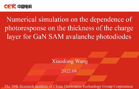
D04 – Numerical simulation on the dependence of photoresponse on the thickness of the charge layer for GaN SAM avalanche photodiodes
GaN avalanche photodiode (APD) has important application prospects in the field of solar-blind ultraviolet (UV) detections. The back-illuminated GaN-based detector has been widely studied due to the advantages such as easy integration with readout circuit. Numerical model of GaN APD is established. The influence of the key function layer (charge layer) thickness on the device […]
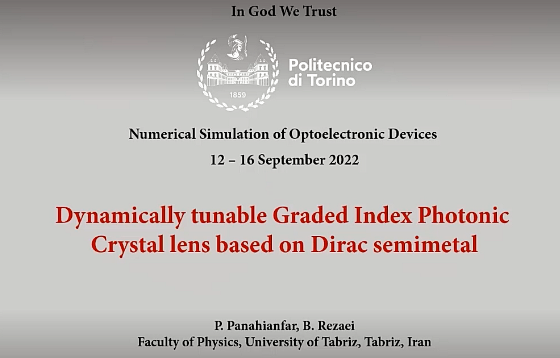
P14 – Dynamically tunable Graded Index Photonic Crystal lens based on Dirac semimetal
In this paper, we design a graded-index photonic crystal based on Dirac semimetals and simulate the light propagation in the proposed structure using two-dimensional finite-difference time-domain method. The numerical results indicate that the designed GRIN PC has focusing capability for incident light at terahertz frequency range, and its focal distance can be tuned through changing […]
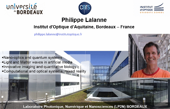
MM01 – Rigorous modal analysis of micro or nanoresonators
The most general motion of a system is a superposition of its normal modes, or eigenstates. We report our recent developments of a rigorous modal analysis of electromagnetic resonators, which is accurate even for geometries that have not been analyzed so far, e.g. 3D resonators made of dispersive media and placed in non-homogeneous backgrounds (on […]
LED03 – RGB LED active region design and optimization with Genetic Evolution Algorithm
Multi-quantum-well (MQW) LED is a complex distributed system with strong interaction between two opposite carrier flows, electrons and holes. For both types of carriers, the carrier injection into each QW depends on transport conditions across the whole active region (AR) and is affected by capture-recombination balance in all active QWs. Multi-color LEDs with different types […]
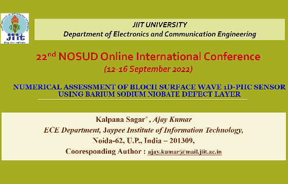
P19 – Numerical Assessment of Bloch Surface Wave 1D-PhC Sensor using Ba2NaNb5O15 Defect Layer
In this paper, a top defective layer of Barium sodium niobate (Ba2NaNb5O15) material of nanometer range thickness is used to confine Bloch surface mode at the upper interface of the proposed structure. For a 1275 nm operating wavelength, the structural characteristics are intended to stimulate a BSW at the top interface. Wavelength interrogation, angle interrogation, […]
LED02 – Carrier Transport in Multi Colour Deep Ultraviolet Light Emitting Diodes
Deep ultraviolet (DUV) light emitting diodes (LEDs) and lasers are enabled by high band gap Aluminium Gallium Nitride (AlGaN). The efficiency of recent multi quantum well (MQW) DUV emitters is still in the percent range which can be in part attributed to the hole injection. The hole injection and the carrier distribution in the high […]
LD12 – Study of reflectivity and resistance properties of p-type distributed Bragg reflectors with composition graded interfaces
In this work, the reflectivity and series resistance of the p-type distributed Bragg reflectors (DBRs) in vertical cavity surface emitting lasers (VCSELs) under the different thickness of composition graded interface layers, Al composition of the high Al composition layers, Al composition of the low Al composition layers, and the number of DBR periods are simulated […]
N05 – Effect of Poole-Frenkel emission on electroluminescence in quantum dot light emitting devices with Nickel Oxide layer
Theoretical analysis of hybrid quantum dot-light emitting devices incorporating CdSe/ZnS core/shell quantum dots and Nickel Oxide (NiO) as hole injection layer (HIL) has been carried out in this work. The replacement of organic HIL such as poly(3,4-ethylenedioxythiophene):poly(styrenesulfonate) (PEDOT:PSS) with solution-processed NiO layer has led to enhancement of current density and luminance in the device by […]
LD01 – Steady states in dynamical semiconductor laser models and their analysis
We present an algorithm for calculating steady states in the dynamic PDE model for SLs admitting gain compression, spatial hole burning, and multilevel carrier rate equations. Presented example simulations rely on 1(time)+1(space)-dimensional traveling-wave- and Lang-Kobayashi-type models.
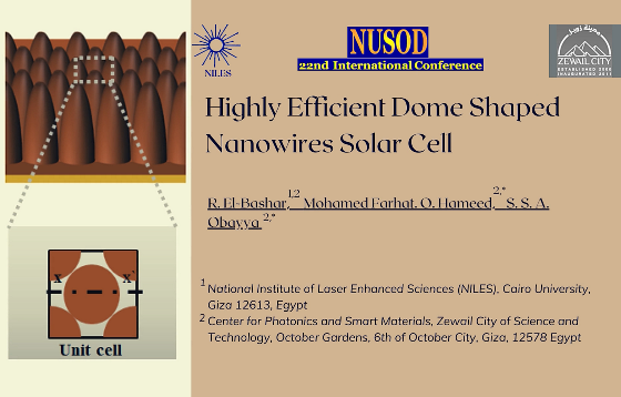
SC05 – Highly Efficient Dome Shaped Nanowires Solar Cell
The optical characteristics of Si dome-tapered nanowires (NWs) solar cell (SC) are reported and analyzed by using finite difference time domain method. The geometrical parameters are studied to maximize the light absorption and hence the ultimate efficiency and short circuit current density of the reported NWs SC. The dome-shaped NWs show better absorption enhancement than […]
SC03 – Simulation and Optimization of Nano-structured Gratings Alternative of Thin-film Anti-Reflectors for GaAs Solar Cells Conversion Efficiency Improvement
Modern civilization demands energy, and the energy demand is increasing almost every day all over the world. The dependency on conventional energy resources including fossil fuel, oil, gas, coal etc. are not in favor of having sustainable global earth. For this reason, renewable or clean energy is one only option while acquiring energy from the […]
IS09 – Collision Dynamics of Solitons in a Grating Assisted Semilinear dual-core System with Phase Mismatch
The collision dynamics between two counterpropagating moving Bragg grating solitons and their outcomes in a model of semilinear dual-core Bragg-grating coupler with phase mismatch are investigated. The influence of gratings phase mismatch on the collision outcomes is also discussed.
LD06 – Relative intensity noise of injection-locked epitaxial quantum dot laser on silicon
This work investigates the relative intensity noise (RIN) characteristics of quantum dot (QD) lasers epitaxially grown on silicon subject to the optical injection. The effect of threading dislocation (TD), which acts as nonradiative recombination centers in the Shockley-Read-Hall (SRH) process, is considered in the rate equation model. The results reveal that the RIN is enhanced […]
IS01 – Network Authentication with Synchronized Chaotic Lasers
We numerically study a hardware method for network authentication, where a pair of matched (twins) chaotic lasers generate the same chaos when they synchronize, being subject to the same optical injection from a third chaotic laser. One of the lasers is in the secure environment, the other in the unsecure environment, and authorization is granted […]
N09 – Beam shaping using a chain of photonic nanojet induced plasmonics
Photonic nanojet arises from a microcavity leading to high electric field. On the other hand, metal nanoparticles (NPs) lead to high field due to localization in small volumes. In this work, PNJ from an array of cavity induced plasmon resonances has been studied. The sharp profile of the PNJ has been observed by the inclusion […]
LD09 – Simulation of the Spectral Behavior in High-Power Distributed Feedback Lasers above Threshold
We report on the simulations of mode hopping behavior in semiconductor distributed feedback lasers with asymmetric facet reflectivities above threshold and its dependence on the phase between the grating and the high reflective facet.
IS05 – Thermal crosstalk mitigation in a dual-drive Mach-Zehnder Modulator
Dual-drive, PIN-diode based Mach-Zehnder modulators are pivotal for power-efficient and cost-effective CMOS compatible optical transceivers with small footprints. However, the basic chip materials have substantial thermal conductance resulting in thermal crosstalk, which eventually deteriorates the modulator performance in terms of bandwidth and data transmission capabilities. In this work, we simulate and analyze the influence of […]
P12 – Design and Simulation of Temperature Sensors Based on Thermo-Optical WGM Shifts in Silica and Non-Silica Glass Microcavities
Sensing applications of dielectric microcavities with whispering-gallery modes (WGMs) have been actively studied in the recent years. Here we investigated theoretically temperature microsensors based on different glasses, including common silica glass, as well as special germanate, tungsten-tellurite, arsenic sulfide and arsenic selenide glasses. We developed numerical model describing sensing characteristics of the considered microcavities. We […]

